This paper first analyzes the absorption mechanism and common texturing methods used to improve the absorption efficiency of silicon-based solar cells, while classifying and explaining the current mainstream laser texturing techniques. Next, the control methods and texturing effects of key process parameters in laser texturing, as discussed in various studies, are organized, and the influence of surface morphology on the absorption effect of laser-textured microstructures is explained. The research progress on chemical post-treatment methods for improving the light absorption effect and photoelectric conversion efficiency of laser-textured polycrystalline silicon surfaces is summarized.

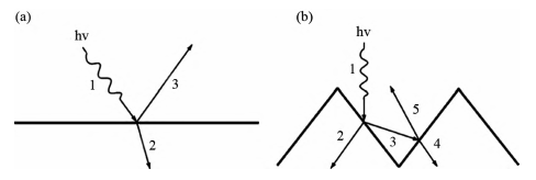
Figure 1 The influence of surface texture on incident light absorption
Currently, most solar cells are made from monocrystalline silicon or polycrystalline silicon. Monocrystalline silicon solar cells have higher photoelectric conversion efficiency, while polycrystalline silicon solar cells require lower raw material purity and have a broader supply, making them much more cost-effective than monocrystalline cells, as shown in Table 1. From an economic perspective, polycrystalline silicon solar cells offer greater future market share and development potential.
Table 1 Comparison of experimental efficiency and performance between monocrystalline silicon and polycrystalline silicon solar cells (data taken from the U.S. Renewable Energy Laboratory - NREL)
| Cell Type | Maximum Efficiency under Non-concentrated Conditions (%) | Maximum Efficiency under Concentrated Conditions (%) | Advantages | Disadvantages |
| Single Crystal Silicon | 25.0 | 27.6 | High efficiency, and long service life | High cost |
| Polycrystalline Silicon | 21.3 | - | Low cost, simple to manufacture | Low efficiency |
The technology of micro-texturing the surface of polycrystalline silicon solar cells is commonly referred to as surface texturing technology. Commonly used texturing methods include organic grooving, chemical etching, reactive ion etching, plasma etching, and laser etching. These methods reduce the surface reflectivity of polycrystalline silicon wafers, but each has inherent drawbacks. For example, the mechanical grooving has a deep groove depth, making it unsuitable for processing thin substrate silicon wafers. The light-trapping microstructure created by chemical etching has a relatively small depth-to-diameter ratio and a limited number of light reflections, and it also causes environmental pollution. Reactive ion etching technology takes a long time and has high production costs.
Laser etching technology is a non-contact process characterized by flexibility, environmental friendliness, and being pollution-free. Laser etching is also referred to as laser surface texturing or laser surface texture, and in the field of polycrystalline silicon solar cells, it is commonly known as laser texturing. This article primarily uses the term laser texturing to describe it. Laser texturing technology involves directly or indirectly etching the surface of polycrystalline silicon wafers using a laser under optimal parameters to create a pyramid-shaped microstructure. Generally, the thickness of an untextured silicon wafer ranges between 400 and 1,000 nm. The average reflectivity is around 35% when exposed to light with wavelengths between 100 and 200 nm. After laser surface texturing, the reflectivity of the polysilicon surface decreases by 10% to 20%, depending on various factors, which influence the process both before and after texturing.