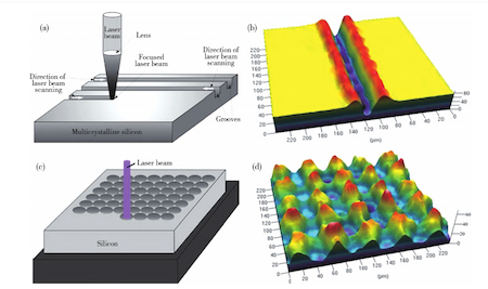
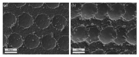
As shown in Figure 11, laser processing can be categorized into continuous and pulsed types based on the working principle. From a macroscopic perspective, laser texturing of polycrystalline silicon wafers can produce various surface patterns, such as grooves, pits, cross-shaped structures, and mixed morphologies, depending on the working principle. Different surface patterns lead to variations in light absorption. Wang Xuemeng and colleagues used a 1064 nm semiconductor-pumped Nd pulsed laser to etch boron-doped P-type polycrystalline silicon wafers, designing two new surface texture structures, as shown in Figure 12. Figure 12a shows a parallel groove array, while Figure 12b is based on the same array, but with adjusted laser parameters to generate continuous pits within the grooves, forming a "groove-pit" hybrid structure. This "groove-pit" hybrid structure is a two-dimensional light-trapping design with a larger surface area and superior light-trapping performance compared to the one-dimensional groove structure. Experiments show that the "groove-pit" hybrid structure offers superior overall performance, with the optimal reflectivity after final treatment reaching 10%.

Figure 11 (a) Working principle of continuous laser texturing (b) Common groove morphology of continuous laser texturing

Figure 12 (a) SEM image of polysilicon parallel groove array textured surface (b) SEM image of polysilicon groove-pit mixed structure textured surface
Microscopic features such as the depth, width (diameter), cross-sectional shape, aspect ratio, and other factors of the microstructure on the laser-textured surface are also crucial for the light trapping properties of polycrystalline silicon wafers. A well-textured surface structure increases the optical path of incident light within the microstructure, thereby enhancing light trapping and improving the anti-reflective effect. Dobrzanski and others used a 50W Nd laser to perform surface groove texturing on boron-doped p-type polysilicon wafers at a wavelength of 1064nm. They etched grooves of varying depths (20µm, 40µm, 60µm, and 80µm) using different laser parameters. Among these, parallel grooves with a spacing of 50µm and an average depth of 40µm yielded the best overall results.
Similar to the study by Dobrzanski and others on the effect of continuous laser etching grooves at varying depths on the reflectivity of the textured surface, Abbott and others investigated the pits ablated by a pulsed laser and etched at different depths (10µm, 20µm, 30µm, 40µm, 50µm) and their impact on the optical properties of the final textured surface. Studies have shown that deeper pits on the surface reduce reflectivity, but they often contain residual ablation debris, which can degrade the electrical properties of the texture. On the other hand, shallow or widely spaced pits reflect more light, but this results in a decline in the optical properties of the texture.
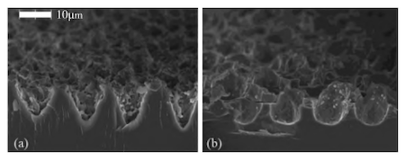
Kim and others altered the cross-sectional groove shape of the textured surface to analyze the light trapping effect on polycrystalline silicon wafers. They used a 355nm ultraviolet laser to create the V-shaped grooves shown in Figure 13a, and a 1064nm fiber laser to create the U-shaped grooves shown in Figure 13b. After texturing and etching, the densely packed V-shaped texture created with the 355nm ultraviolet laser captures photons more effectively than the U-shaped texture created with the 1064nm fiber laser.
Research by Kunxia Wang and others shows that for surfaces with the same size and uniformity, the light trapping property of a V-shaped textured surface is better than that of a U-shaped textured surface. This result closely mirrors the findings of Kim and others.

Figure 13 Samples textured by (a) UV laser and (b) fiber laser and etched by NaOH
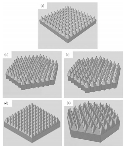
Hua and others developed several textured structures, as shown in Figure 14: square array cones (Figure 14a), close-packed cones (Figure 14b), closely packed hexagonal pyramids (Figure 14c), closely packed rectangular pyramids (Figure 14d), and close-packed triangular pyramids (Figure 14e). They studied the effects of factors such as geometry, density, and vertex angle of the silicon front texture on solar light absorption. The simulation results show that when the pyramid vertex angle is less than 100°, the tapered structure on the front side of the silicon wafer exhibits the lowest absorption rate. However, the triangular pyramid structure performs the best, achieving a light absorption rate of over 90% across the 640-1080 nm wavelength range.
Studies have shown that absorptivity varies with changes in texture shape. Peng She and others investigated the different light trapping effects achieved by textured microstructures at varying aspect ratios, using a 5W quasi-continuous semiconductor laser to process the surface of p-type polysilicon. When the aspect ratio of the microstructure obtained by laser etching is 1:2 (with an etching depth of about 50µm and width of 100µm), the anti-reflection effect is poor, and the average surface reflectance in the 300-1100 nm range is 18.2%. However, when the aspect ratio is 2:1 (with a depth of 60µm and width of 30µm), the light trapping effect improves significantly, and the average surface reflectance drops to 10.2%. Table 3 shows that both macroscopic and microscopic surface microstructure morphology affect texturing quality and light trapping efficiency. The texture quality depends on the type and parameters of the laser. Continuous lasers are suitable for engraving grooves, which can be arranged in parallel or intertwined patterns to form a textured structure. In contrast, pulsed lasers, due to their discontinuity, create textures consisting of pits arranged at different spacings. The depth and diameter of the microstructure increase proportionally with the pulse repetition frequency and single pulse energy. Additionally, increasing the laser power results in a greater change in depth than in diameter. When determining pit size, the pulse repetition frequency is more decisive than the single pulse energy. Research has shown that various structures can be created on the surface of polycrystalline silicon wafers by adjusting laser and process parameters.
Table 3 Effect of typical textured surface morphology on the light absorption effect of Polycrystalline Silicon Wafers
| Source | Macromorphology (Parallel, Dotted, Composite) | Micromorphology (Depth, Aspect Ratio, Cross-section) | Reflectivity (%) | Reflectivity After Chemical Etching (%) | Photoelectric Conversion Efficiency (%) |
| Xuemeng Wang and others | Composite morphology | -- | 6.90 | 10 | 15.70 |
| Parallel groove | -- | 6.30 | >10 | -- | |
| Dobrzanski and others | Parallel groove | Depth of 40μm | 21.21 | -- | 11.93 |
| Point array | Depth of 40μm | 16.38 | -- | 12.67 | |
| Abbott and others | Point array | Depth of 30μm | -- | <20 | 18.40 |
| Kim and others | Point array | V-shaped cross-section morphology | 8.60 | 13.20 | -- |
| Hua and others | -- | Three-school tapered surface morphology | <10 | -- | -- |
| Peng She and others | Point array | Aspect ratio 2:1 | 10.20 | -- | -- |
Note: "--" means this content is not indicated in the literature.

Figure 14 Various suede structures